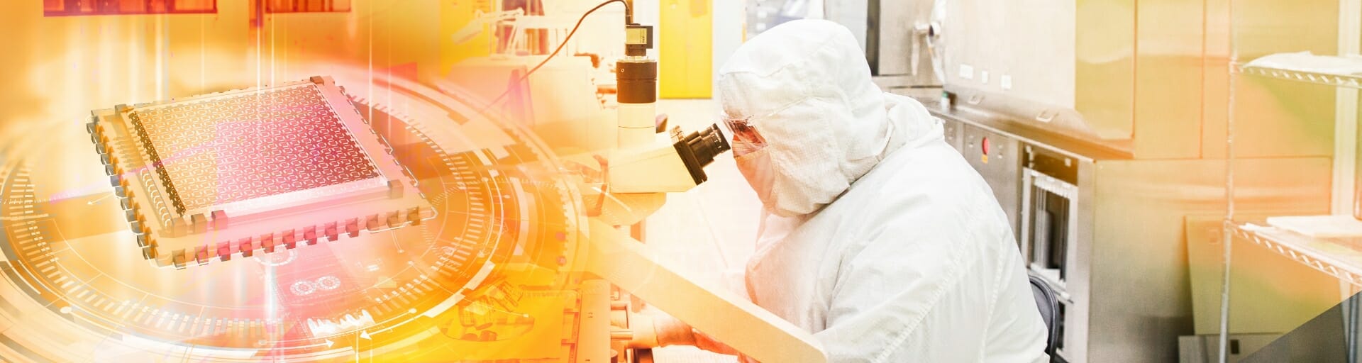
Research and development
Driving microelectronics innovation and industrial growth
ASU’s approach to microelectronics R&D is expressly focused on industry and defense needs. Through collaboration with enterprises from local to global scales, as well as multiple federal and defense investments and programs, ASU is co-creating the innovation ecosystem needed to ensure a resilient and secure microelectronics supply chain.
ASU designs custom engagements with industry partners to enable scale-ready technological solutions and innovations. And through the Microelectronics Industry Council, ASU is working to solve challenges facing the semiconductor industry in Arizona and beyond. Additionally, ASU is a trusted R&D partner to the U.S. government on defense initiatives, advancing critical microelectronics projects for DARPA and the U.S. Air Force, Army and Navy
Create a customized partnership
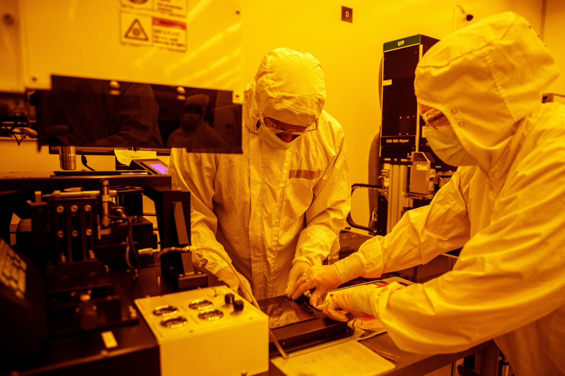
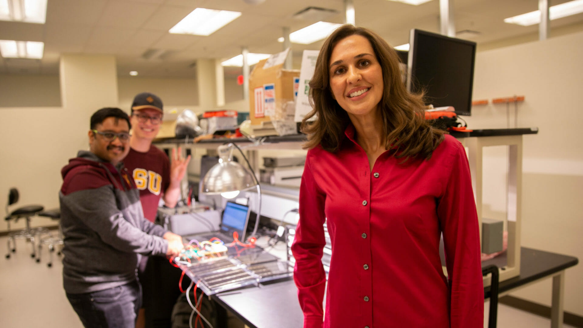
How ASU faculty expertise drives microelectronics innovation
Faculty members at ASU are at the forefront of materials and manufacturing research that promises to dramatically improve microchip performance and enable emerging technologies. ASU researchers are developing ways to mass-manufacture chips using 3D integration — the next field of chip innovation as industry works to meet demands for power, performance, area and cost (PPAC). ASU faculty are also exploring the potential of nanolasers to enable the development of supercomputer capabilities on a single chip. Additionally, ASU researchers are leading experts in heterogeneous integration to increase chip capabilities and open up new technological frontiers in aerospace and defense, autonomous vehicles, sensors, wearable devices and sustainable energy.
ASU Faculty expertise extends across the full spectrum of microelectronics design and production, from foundational, theoretical science through development of applied manufacturing solutions.
Modeling and Testing
Materials
Devices
Circuits
Systems
Manufacturing
Key research focus areas

Power electronics
Wide-bandgap materials like diamond, GaN and SiC provide improved electrical performance to enable the next generation of high-speed data and communications, smart power grids, and autonomous vehicles.
Wireless and mixed-signal circuit design
New materials and devices with high-power and high-speed capabilities allow for new designs that improve chip performance. With smarter design, chips in small electronic devices could crunch data at speeds that require a room-sized computer today.
Memory devices and architectures
Combining computational and memory components will improve chip efficiency. New architectures will allow devices to use high-efficiency machine learning models.
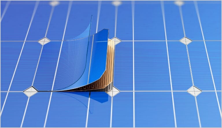
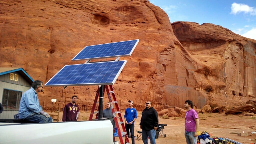
Solar energy and batteries
Solar energy and batteries are key components of sustainable energy systems ranging from the power grid to electric vehicles. Electronics that can share information across the grid will tell us how much energy is available from a source, allow us to draw from renewable sources efficiently and enable more widespread use of renewable energy.

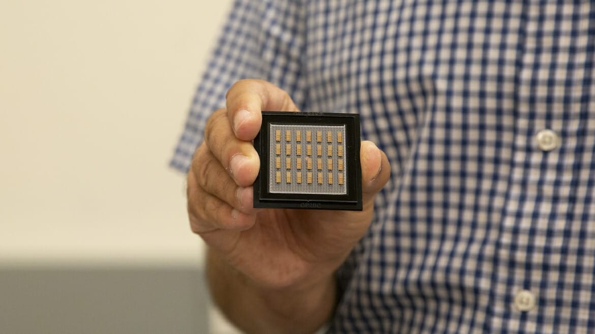
Packaging and heterogeneous integration
The future of semiconductor packaging will integrate displays, batteries, high-frequency communications and more into systems with unprecedented computational and functional density. The next technological leap will leverage new materials, devices architectures and advanced packaging innovations to meet demands for power, performance, area and cost.
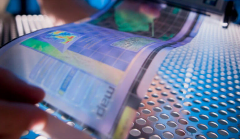
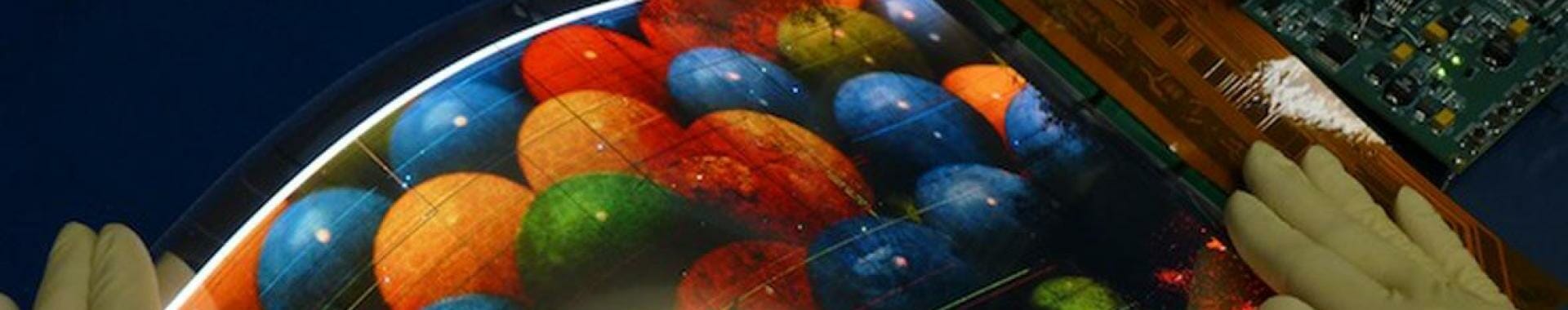
Flexible electronics and displays
Flexible electronics and displays offer potential to improve solar power efficiency, enable bioelectronic and wearable technologies, and create miniature antennas for wireless devices. Further applications include flexible energy storage for powering fully flexible devices and alternative ways to harvest energy from ambient heat, movement and friction.
Science and Technology Centers at the forefront of microelectronics innovation
Leveraging funds from Arizona’s New Economy Initiative, ASU has developed five new Science and Technology Centers (STCs) that bring together faculty, industry professionals, entrepreneurs and students to take big ideas from the lab to market. STCs focus on solving major industry, defense and environmental challenges, leveraging cutting-edge research and expertise in microelectronics to advance research and innovation.
AMPED STC: Advanced Materials, Processes and Energy Devices
Advances new materials and devices for solar, battery and power electronics for the broad electrification of the energy sector.
MADE STC: Manufacturing, Automation and Data Engineering
Creates foundational manufacturing technologies and methods using process science and engineering, robotics and automation, and data analytics, cyber and AI.
ACT STC: Advanced Communications Technologies
Drives innovation in physical information systems and sensing and communications solutions to meet the emerging demands of high-bandwidth applications.
PERFORM STC: Human Performance
Develops novel technologies to enhance physical and cognitive performance and improve medical prevention and interventions.
EXTREME STC: Extreme Environments
Addresses challenges of growing population centers by engineering resiliency into transportation, energy, water and materials systems that impact future cities.
ASU microelectronics centers, labs and initiatives
ASU’s microelectronics R&D footprint is expansive, comprising numerous centers, labs and initiatives facilitating the work of diverse research teams working to develop industry-relevant solutions.

Adaptive Intelligent Materials and Systems Center
leverages multidisciplinary research for development of a unified theoretical foundation for integrated intelligent systems. Research foci include multiscale modeling from nano to structural scale; intelligent design and optimization; and multifunctional materials and adaptive systems.

Materials of the Universe (MotU)

Center for Embedded Systems (CES)
A collaboration between ASU, Southern Illinois University, the National Science Foundation and industry that focuses research on technologies that enable sensing, communications, computing and control in everyday things.
Center for Photonics Innovation
Integrates a broad spectrum of research topics ranging from fundamental study of photon-matter interactions to practical optical sensors for medical and biological applications.

Compact X-ray Free Electron Laser (CXFEL)
Enables research on X-ray pulses so short that they outrun all X-ray damage processes, allowing scientists to conduct novel science to explore the structure and dynamics of nature and materials as never before.
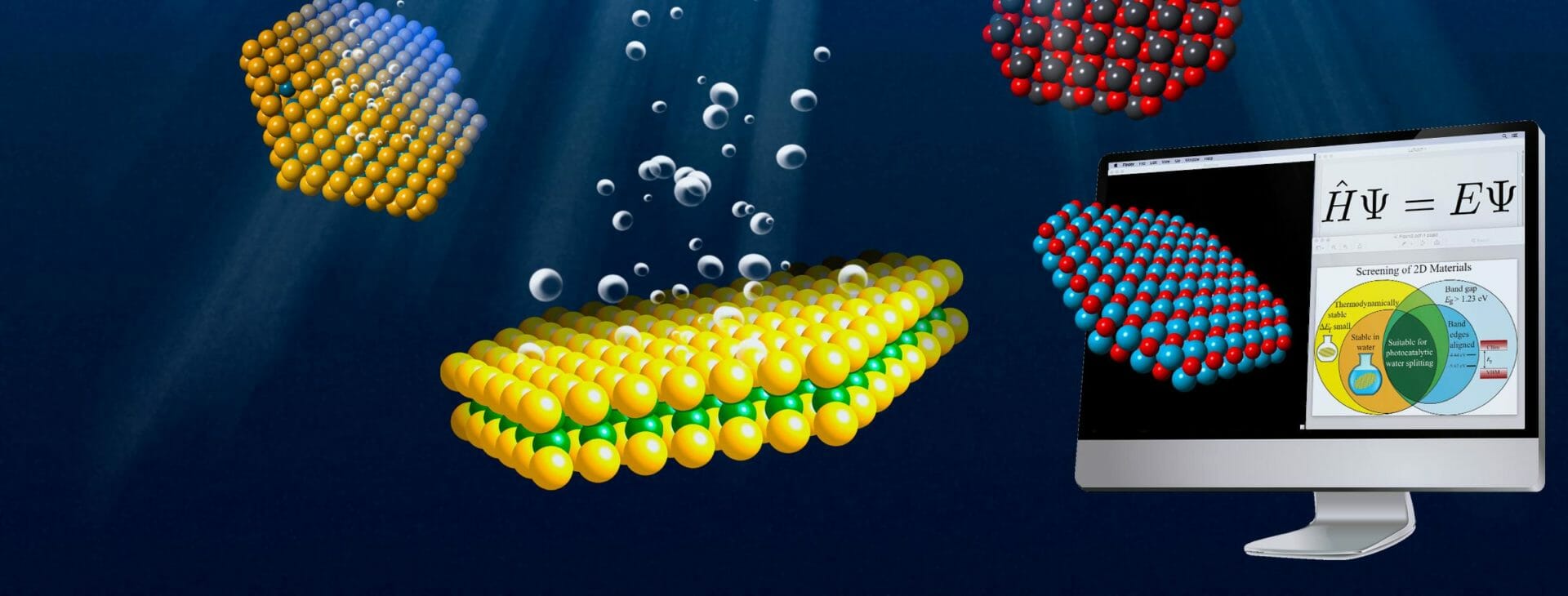
Computational Materials Design Lab
Focuses on atomistic simulations of complex surfaces and interfaces. The Lab develops quantum mechanical simulations and molecular dynamics simulations to push the boundaries of knowledge in nanomaterials, 2D materials and surface dominant-phenomena.
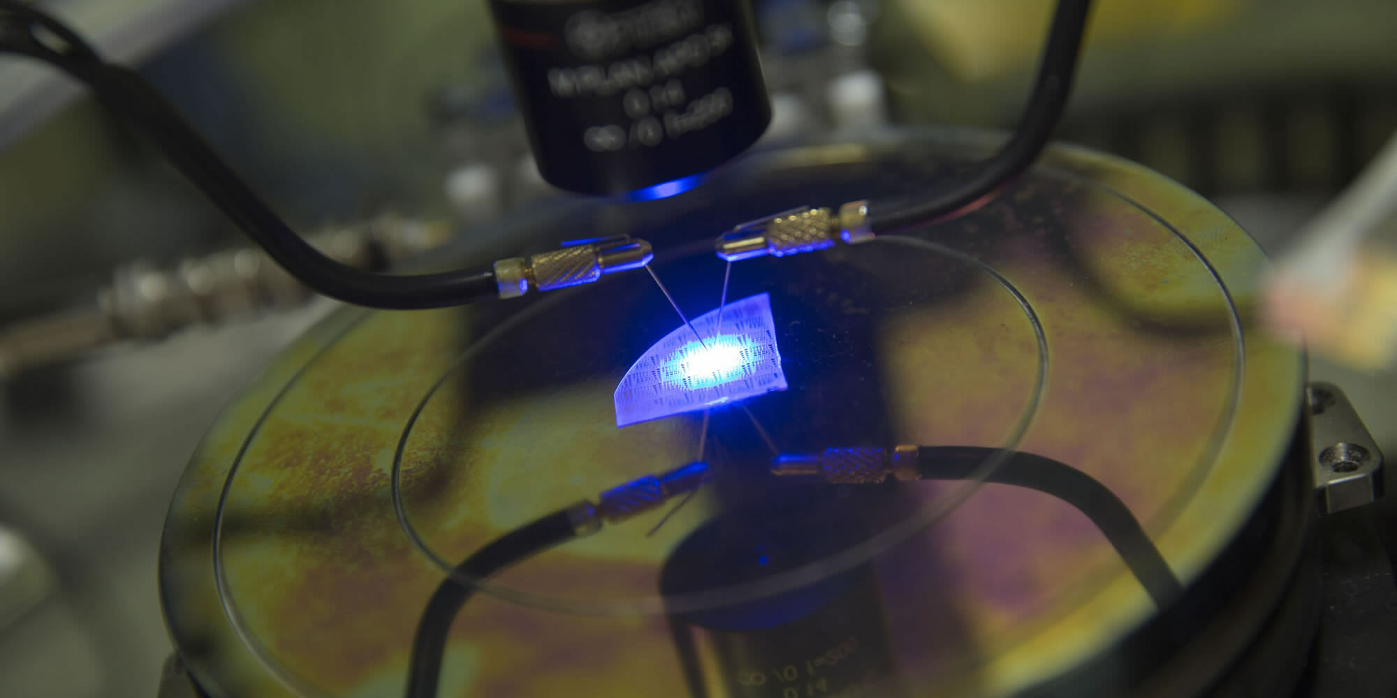
Flexible Electronics and Display Center
Provides comprehensive flexible electronics capabilities that bridge the high-risk, resource-intensive gap between innovation and product development in an information-secure environment. Backplane electronics design, fabrication, test and integration capability are located at the ASU Research Park.

Nanotechnology Collaborative Infrastructure Southwest (NCI-Southwest)
Serves as the Southwest hub of the National Nanotechnology Coordinated Infrastructure (NNCI).
NSF Engineering Research Center for Quantum Energy and Sustainable Solar Technologies (QESST)
Advances education and research around novel, efficient photovoltaic technologies to meet the growing demand for clean energy.

Sensor, Signal and Information Processing Center (SenSIP)
A National Science Foundation Industry/University Cooperative Research Center that develops a broad array of digital signal processing, imaging and communications algorithms for sensor network technologies including those used in chemical sensors, Internet of Things (IoT), health monitoring, cell phones, security and radar systems.
Featured research projects
Poised to help close the microchip manufacturing gap
Our focus areas relevant to the CHIPS Act include investments, facilities, unique tool sets and one of the science and technology centers that are in line with this.
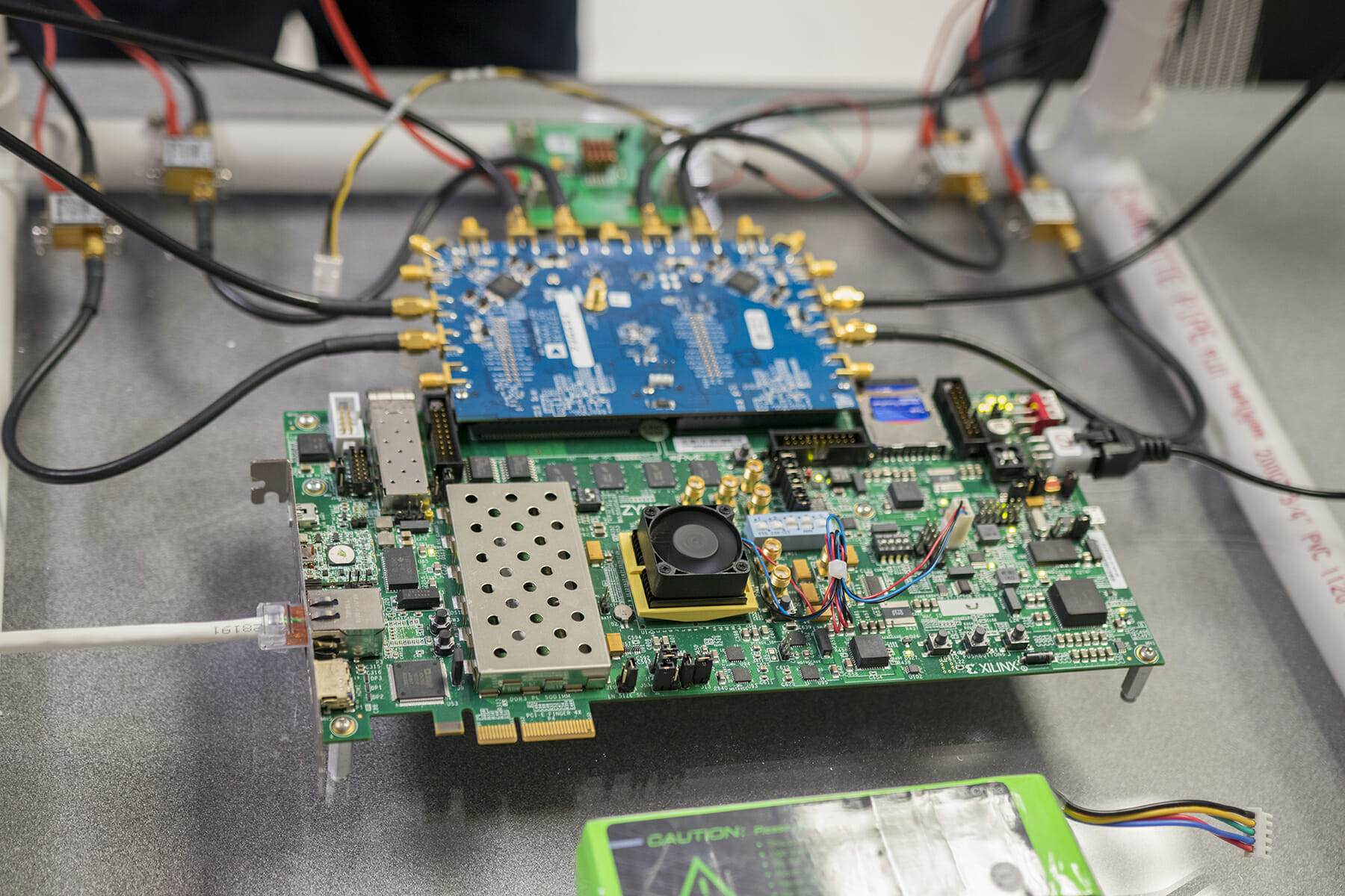
Developing the computational architecture of the future
ASU researchers lead a $17 million DARPA effort to expand computing technology capabilities and energy efficiency.
Automated design for faster, lighter electronics
ASU engineer Jennifer Kitchen received an NSF CAREER award to automate design processes for power electronics.
Enhancing the performance of wireless systems
A Young Investigator Award from the Office of Naval Research advances Saeed Zeinolabedinzadeh’s research.
ASU researcher adds new dimension to semiconductor manufacturing
An NSF CAREER award supports Bruno Azeredo’s work to mass produce nanoscale semiconductor devices in 3D.